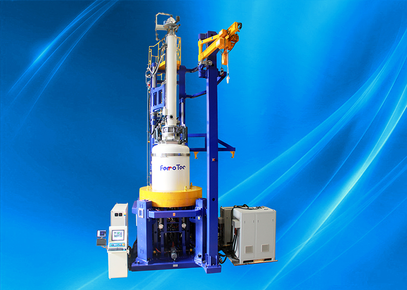

Recently, Shanghai Hanhong Precision Machinery Co., Ltd. reported again that the 12 inch semiconductor single crystal furnace (ft-cz3212b) began to be put into use in batch. The equipment can stably massively produce high-quality large-diameter crystal rods, which also marks the key effect of large-scale and industrial layout of 12 inch silicon wafers, and a major breakthrough in the most core pulling crystal link. It can be said that this will usher in a qualitative leap in the field of domestic semiconductor silicon materials, and the industrialization process of 12 inch silicon wafers will take a new step.
Shanghai Hanhong semiconductor fully automatic 12 inch semiconductor single crystal furnace has reached a new height in terms of uniformity and defect density, breaking through the industrial pattern that domestic crystal silicon material growth equipment, especially large-diameter crystal silicon material growth equipment, has been monopolized by foreign large-scale enterprises for a long time. All data and indicators have reached the international advanced level, filling the blank of the domestic semiconductor crystal pulling equipment , and laid a good foundation for domestic high-quality large-diameter silicon chip research and development and industrialization.

Shanghai Hanhong adheres to R & D innovation and relies on Ferrotec group's leading core technology in the field of semiconductor silicon material equipment. In the R & D process, project members fully understand the production needs of customers, and maintain a high degree of equipment design sensitivity. After repeated experiments and improvements in the procurement, outsourcing, quality, manufacturing and other aspects, the company finally focuses on the precision of each team With close cooperation, we will further ensure the stability and reliability of equipment operation.
It is reported that compared with the mass production progress of 8-inch domestic silicon wafers, 12 inch domestic silicon wafers are far from the stage of capacity release, and the supply is far from enough compared with the huge demand. It is preliminarily estimated that China's chip manufacturing capacity is expected to reach 30% of that of the world by 2020. At that time, China's 12 inch silicon chip production capacity and chip foundry production capacity are seriously mismatched. In addition to the gap between supply and demand, the quality of 12 inch silicon wafers in China also needs to be improved urgently. This indicates the feasibility and necessity of mass production of large diameter single crystal furnace. Shanghai Hanhong 12 inch single crystal furnace will break the difficult situation of insufficient production capacity of China's 12 inch SOI substrate, and will gradually change the situation that China's 12 inch silicon substrate is heavily dependent on imports.
The downstream market of semiconductor monocrystalline silicon wafer is promising, and the demand for 300mm silicon wafer continues to grow. Semiconductor chip manufacturing technology follows Moore's law. The growth and development of different sizes of silicon chip market rotate, and the whole silicon chip develops along the trend of large size. The larger the diameter of the monocrystalline silicon chip is, the more integrated circuits can be made, and the lower the cost of the chip is. The larger the size of silicon wafer, the higher the benefit.
Shanghai Hanhong's batch production line of 12 inch semiconductor single crystal furnace represents that its technology and quality level have reached the world's advanced level and are widely recognized by the market. It can keep pace with the advanced enterprises and equipment in developed countries and fill in the technical gap in this field in China. While greatly promoting the large-scale development of the domestic semiconductor industry, it has also injected new opportunities for the development of Shanghai Hanhong, laying a solid foundation for the company to continue to rise to "high, precise and sharp" in the semiconductor equipment industry.