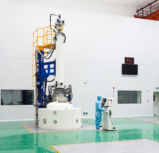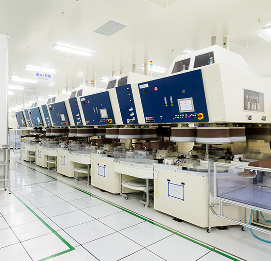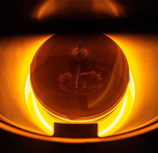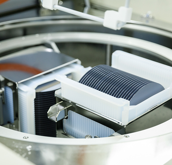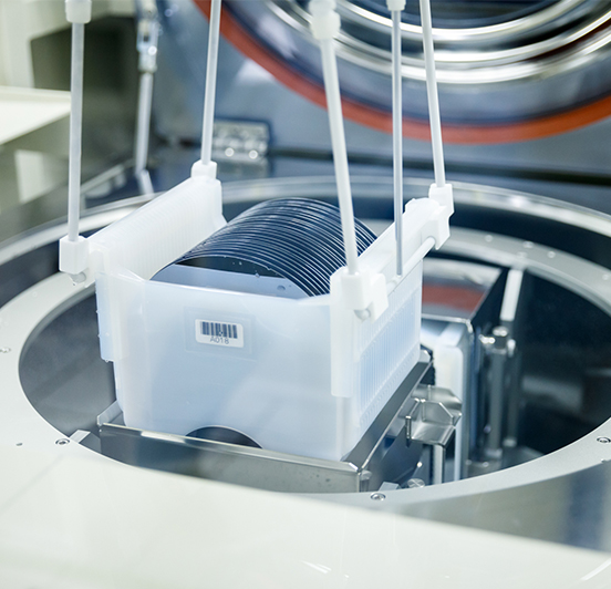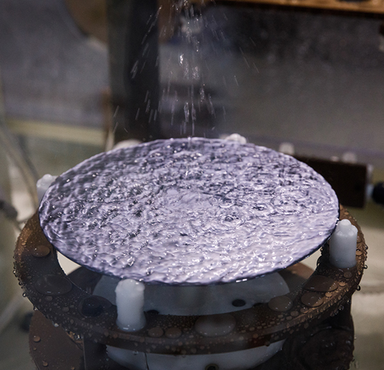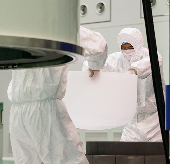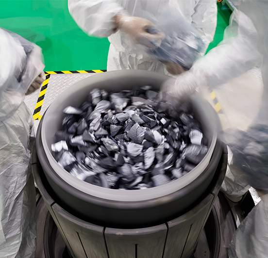
Based on which Ferrotec researched and developed high processing technology for 8” wafer with independent intellectual property right through introduction, absorption and innovation of technology. Ferrotec adopts Japanese semiconductor wafer processing equipment like 3-way lapping machine, non-basket final cleaning process, AGV transport system, roof-carrying system, and also introduced full-auto polishing line integrating tape mounting, lapping and polishing, and applies semiconductor single crystal furnace independently manufactured by Ferrotec (China). Along with its growing production capacity, Ferrotec (China) gradually possesses production ability of 8” and 12” wafers, which paves the way for Ferrotec (China) to build internationally advanced big size wafer R&D base for innovation and industrialization, and strives to become the first supplier in China of 200mm semiconductor wafers and 300mm semiconductor wafers with monthly production capacity of 450,000 pieces of 200,000 pieces respectively.
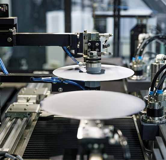
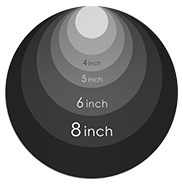
Our silicon wafers have good control in resistivity, flatness, particle, COP and metal contamination, etc. They are mainly used in various fields such as memory, logic integrated circuits, power devices, sensors, etc., and can be directly applied to CMOS, EPI, SOI, MEMS and other silicon-based substrates, which makes up for 8" and 12" semiconductor single crystal wafer demand of the integrated circuit industry, automotive, computer, consumer electronics, communications, industry, medical treatment, and guarantees the national safety supply of silicon wafers and the integrity and stability of the integrated circuit industry chain, all of which are of great significance to the development of China's semiconductor industry.